铍铜合金
高性能合金凭借卓越的导电性能与抗应力松弛特性,为个人电脑及手持电子设备中的连接器、弹簧与开关提供高可靠性保障。
获取铜铍合金的更多技术参数
Get additional information about copper beryllium alloys.
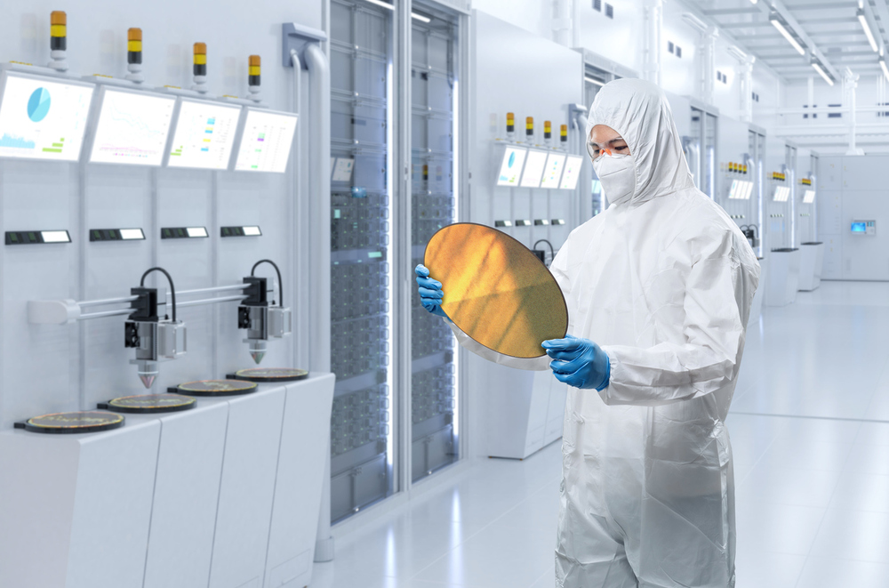
蒸发材料
这类产品可助力物理气相沉积(PVD)工艺实现优异的蒸发性能,产品品类涵盖起始源材料、金属块、金属粒、金属片、坩埚内衬以及无机化学品 inorganic chemicals 。想了解更多相关信息,可查阅 evaporation materials.
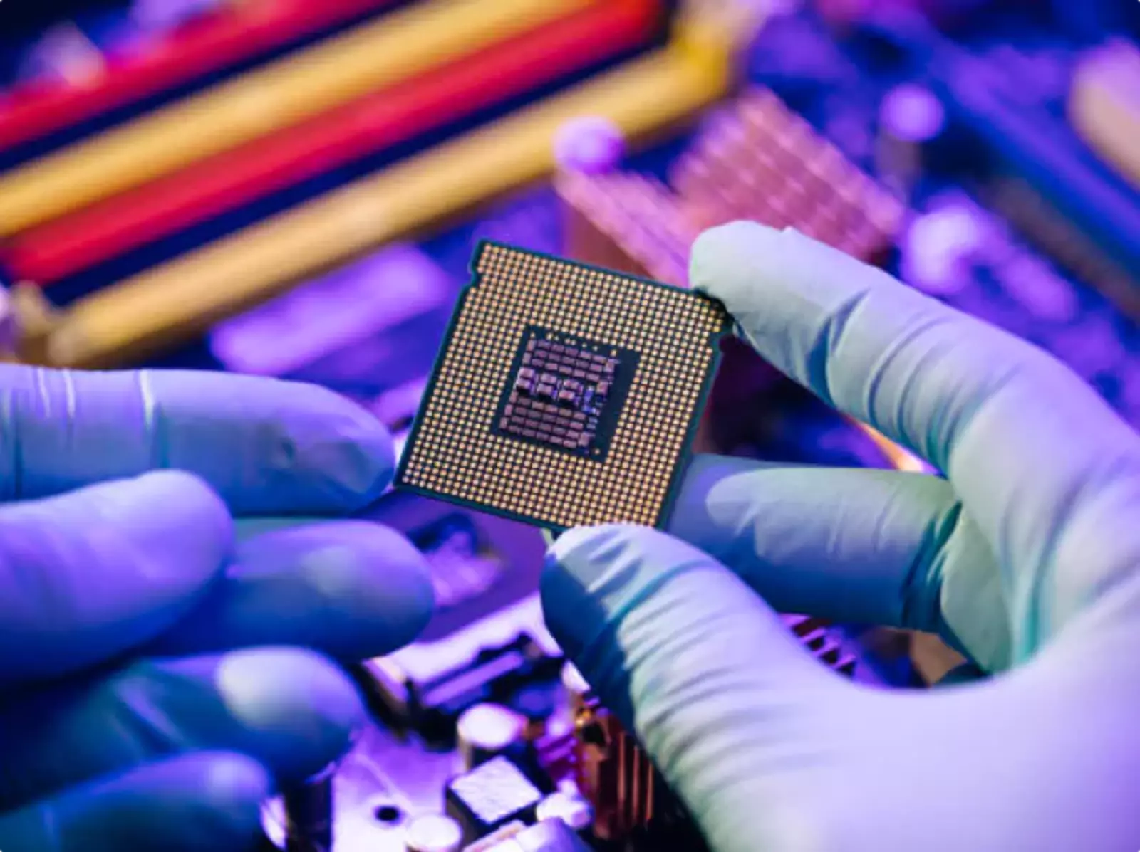
高性能溅射靶材
我们提供品类全面的溅射靶材,其涵盖的元素占元素周期表的 70% 以上,可满足客户在材料种类、尺寸规格、结构设计及形态配置等方面的多样化需求。想了解更多相关信息,可查阅溅射靶材详情。 sputtering targets
金属基复合材料
服务于XY工作台及高速运动部件的高比模量材料,广泛应用于引线键合、光罩检测等精密工艺场景。
深入了解金属基复合材料技术
Read more about metal matrix composites.
原子层沉积(ALD)的前驱体材料
适用于先进半导体应用的原子层沉积(ALD)用固态前驱体材料。想了解更多相关信息,可查阅ALD 前驱体详情。 ALD precursors.
PVD 耗材
适用于薄膜沉积工艺的各类耗材产品,包括背板、坩埚内衬以及靶材键合胶等。想了解更多相关信息,可查阅PVD 耗材详情。 PVD consumables.
工程陶瓷
氧化铝陶瓷以其优异的热稳定性、尺寸稳定性及极低的热膨胀系数(严格公差范围内),成为半导体制造工艺的经济高效之选。
探索氧化铝陶瓷材料技术详情
Learn more about alumina ceramics.